Geon has developed a Frequency Estimator IP which can perform FFTs of configurable bin size to estimate the frequency of an RF input. The IP achieves high precision while consuming few resources. Development and integration of the IP was accelerated using Geon’s FINS (Firmware IP Node Specification) toolchain. The development process and its advantages are elaborated below.
Development Process
The following list summarizes the different phases of this development process:
1. Develop an IP using FINS and validate it using the FINS-generated VHDL testbench
2. Construct a working baseline ZCU102 platform including an FPGA design and SD card image
3. Design a mechanism for moving data between software and the FINS IP
4. Integrate with a software testbench using the FINS Software Package
1: IP Design with FINS
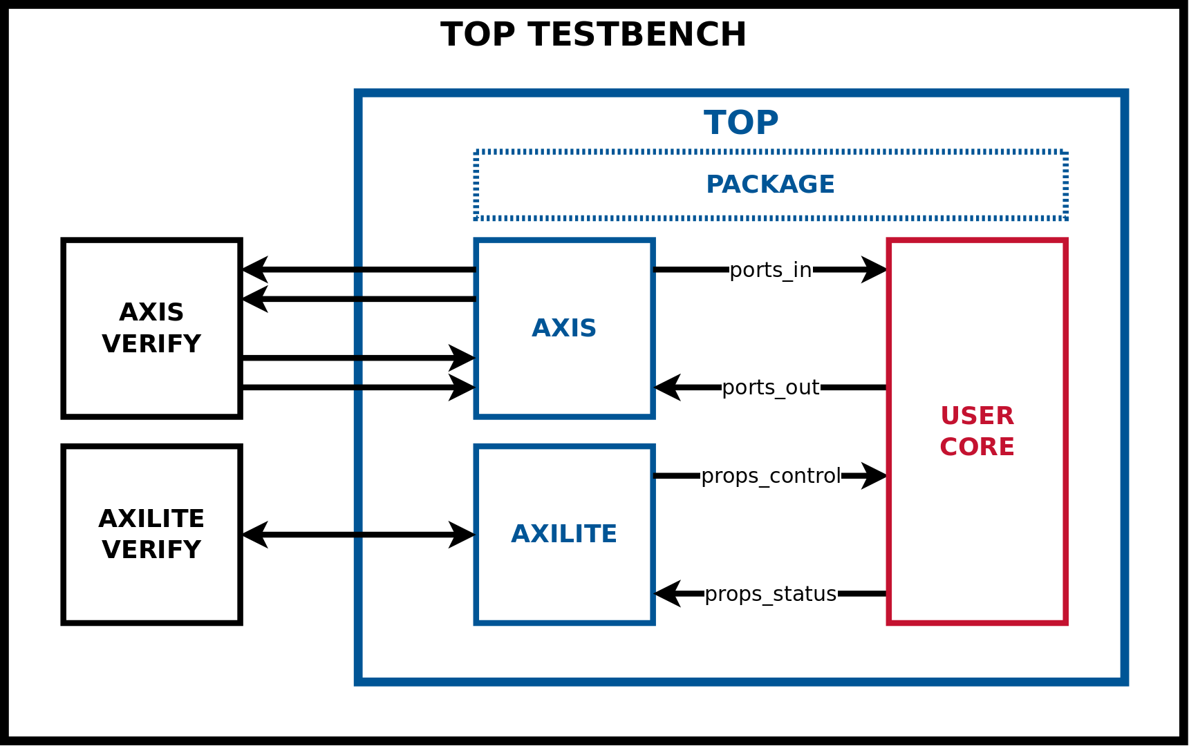
During the IP development stage, FINS generates a VHDL harness that simplifies the port and property interfaces to the core logic module. The Frequency Estimator IP uses standard AXI-Streaming interfaces for inputs and outputs. The Frequency Estimator does not have any properties (FINS Software Registers via AXI4-Lite), but if it did, FINS would generate all of the necessary AXI4-Lite logic, and expose very basic property-access signals to the core logic module.
Once the interface to the IP was defined, FINS was leveraged to generate a simulation testbench for the IP. A FINS-generated testbench includes basic port and property verification and gives the user clear entry points for input/output data and further verification logic.
This simulation testbench was used in an iterative manner during development. Once simulation testing was complete, it was time to move on to a true hardware test.
2: Baseline ZCU102 Design
We chose the ZCU102 Evaluation Board as our test hardware because it is cutting-edge, industry-standard hardware.
Through the use of both Tcl and PetaLinux, we were able to get a baseline design up and running quickly with relatively low effort. We used Tcl to construct a basic GPIO LED design, applied the petalinux tools to generate an SD card image, and validated the base design by monitoring the GPIO LEDs. We also inserted our FINS Software Package into the PetaLinux project for use in section 4.
3: Data Movement – Software <> FINS IP
At this point, we needed to solve the issue of data transfers in and out of the FPGA. While FINS does not yet have a complete set of tools for DMA automation, its property interface automation is quite robust. So, we decided to use the FINS property interface to manage the software-firmware boundary.
We did this by constructing two highly reusable FINS IPs: sw2fpga_fifo and fpga2sw_fifo. Each of these IPs includes a data_in/out property for moving data to or from the FPGA. These properties can be accessed by name from software to transfer data.
4: Integration with Software
Leveraging the abstractions created in step 3, we developed a software testbench runnning on the Zynq UltraScale+ ARM processor. Using the fins-poke Bash utility, or the FINS Software Package C++ API, data can be written to the data_in property of the sw2fpga_fifo, and frequency estimations can be read from the data_out property of fpga2sw_fifo.
Our validation software used the C++ API to write data to the FPGA, and then used the fins-poke bash utility to validate the results.
Here is a snippet that shows the simplicity of the C++ API:
while (<data incoming>) {
    nodeset.write_safe("sw2fpga_fifo", "data_in", value);
}
And here we read the resulting frequency estimate via Bash:
$ fins-poke -n fpga2sw_fifo data_out
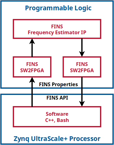
Below is the complete architecture of the Frequency Estimator IP test implemented on the ZCU102 Evaluation Board:
What’s Ahead
Development, testing and integration of the Frequency Estimator IP were simplified and accelerated through the use of the FINS toolchain. The one-time cost of developing the SW-HW FINS IPs will likely be well worth the effort. Not only will these IPs be valuable in future projects, but FINS may eventually provide automation for auto-insertion of these IPs. This will further simplify the process of integrating firmware IPs with software.
FINS “Application” support for Vivado designs will be coming soon and will give the developer even more confidence in an FPGA design before testing in hardware. This additional automation will make it seamless to simulate the full firmware “Application” (in this case: sw2fpga_fifo –> frequency_estimator –> fpga2sw_fifo). Using FINS’ property verification package and a FINS-generated testbench baseline, a developer will be able to simulate the full data path: property writes to drive data into the IP, frequency estimation, and property reads to validate the results.
This project was an exciting one, and our improvements in development process and tooling will enable more exciting projects in the future!